| Description | The LM317 device is an adjustable three-terminal positive-voltage regulator capable of supplying more than 1.5 A over an output-voltage range of 1.25 V to 37 V. It requires only two external resistors to set the output voltage. The device features a typical line regulation of 0.01% and typical load ... |
| Features |
•1 Output voltage range adjustable from 1.25 V to 37 V • Output current greater than 1.5 A • Internal short-circuit current limiting • Thermal overload protection • Output safe-area compensation 2 Applications • ATCA solutions • DLP: 3D biometrics, hyperspectral imaging, optical networking, and spectroscopy • DVR and DVS • Desktop PCs • Digital signage and still cameras • ECG electrocardiograms • EV HEV chargers: levels 1, 2, and 3 • Electronic shelf labels • Energy harvesting • Ethernet switches • Femto base stations • Fingerprint and iris biometrics • HVAC: heating, ventilating, and air cond... |
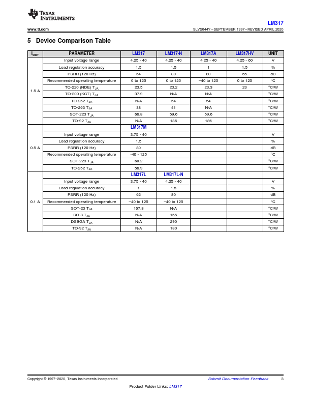
| Datasheet |
|

| Part Number | Description |
|---|---|
 ON Semiconductor |
Positive Voltage Regulator Voltage Regulator – Adjustable Output, Positive 1.5 A LM317, NCV317 The LM317 is an adjustable 3−terminal positive voltage regulator capable of supplying in excess of 1.5 A over an output voltage range of 1.2 V to 37 V. This voltage regulator is exceptionally easy to use and requires only two external resistors to set the output voltage. Further, it employs internal current limiting, thermal shutdown and safe area compensation, making it essentially blow−out proof. The LM317 serves a wide variety of applications including local, on card regulation. This device can also be used to make a programmable output regulator, or by connecting a fixed resistor between the adjustment and output, the ... |
 Kexin |
Linear Integrated Circuit SSMMDD TTyyppee Linear Integrated Circuit LM317DY Ƶ Features ƽ Output voltage adjustable from 1.3V ~ 37V ƽ Output current in excess of 1.5A ƽ Internal short circuit protection ƽ Internal over temperature protection ƽ Output transistor safe area compensation +0.040.21 -0.02 SOP-8 Ƶ Block Diagram INPUT IC 1.50 0.15 1 Vin 2 VOUT 3 VOUT 4 Adj 5 N.C. 6 VOUT 7 VOUT 8 N.C. VREF VADJ PROTECTION CIRCUIT OUTPUT Ƶ Absolute Maximum Ratings (TA=25ć, unless otherwise specified)) Parameter Symbol Rating Input Voltage VI 40 Maximum Output Current IO 1.5 Power Dissipation PD Internal limited Thermal Resistance, Junction-to-Ambient RthJA 190 Thermal Resistance, Junction-to-Case RthJC... |