| Description | The 74ABT08 is a quad 2-input AND gate. This device is fully specified for partial power down applications using IOFF. The IOFF circuitry disables the output, preventing the potentially damaging backflow current through the device when it is powered down. 2. Features and benefits • Supply voltage r... |
| Features |
and benefits
• Supply voltage range from 4.5 V to 5.5 V • BiCMOS high speed and output drive • Direct interface with TTL levels • IOFF circuitry provides partial Power-down mode operation • Latch-up protection exceeds 500 mA per JESD78B class II level A • ESD protection: • HBM JESD22-A114F exceeds 2000 V • MM JESD22-A115-A exceeds 200 V • Specified from -40 °C to +85 °C 3. Ordering information Table 1. Ordering information Type number Package Temperature range Name 74ABT08D -40 °C to +85 °C SO14 74ABT08PW -40 °C to +85 °C TSSOP14 Description plastic small outline package; 14 leads; body... |
| Datasheet |
|

| Part Number | Description |
|---|---|
 NXP |
Quad 2-input NAND gate The 74ABT00 high-performance BiCMOS device combines low static and dynamic power dissipation with high speed and high output drive. The 74ABT00 is a quad 2-input NAND gate. 2. Features and benefits Latch-up protection exceeds 500 mA per JESD78B class II level A ESD protection: HBM JESD22-A114F exceeds 2000 V MM JESD22-A115-A exceeds 200 V Multiple package options Specified from 40 C to +85 C 3. Ordering information Table 1. Ordering information Type number Package Temperature range Name 74ABT00D 40 C to +85 C SO14 74ABT00DB 40 C to +85 C SSOP14 74ABT00PW 40 C to +85 C TSSOP14 Description plastic small outline package; 14 leads; body width 3.9 mm plastic shr... |
 Philips |
Quad 2-input NAND gate PIN NUMBER SYMBOL NAME AND FUNCTION 1, 2, 4, 5, 9, 10, 12, 13 An-Bn Data inputs 3, 6, 8, 11 Yn Data outputs 7 GND Gr... |
 nexperia |
Quad 2-input NAND gate The 74ABT00 is a quad 2-input NAND gate. This device is fully specified for partial power down applications using IOFF. The IOFF circuitry disables the output, preventing the potentially damaging backflow current through the device when it is powered down. 2. Features and benefits • Supply voltage range from 4.5 V to 5.5 V • BiCMOS high speed and output drive • Direct interface with TTL levels • IOFF circuitry provides partial Power-down mode operation • Latch-up protection exceeds 500 mA per JESD78B class II level A • ESD protection: • HBM JESD22-A114F exceeds 2000 V • MM JESD22-A115-A exceeds 200 V • Specified from -40 °C to +85 °C 3. Ordering information Table 1. Ordering information T... |
NXP |
Quad 2-input NOR gate µA PIN NUMBER 2, 3, 5, 6, 8, 9, 11, 12 1, 4, 10, 13 SYMBOL An-Bn Yn GND VCC NAME AND FUNCTION Data inputs Data outputs Ground (0V) Positive supply voltage PIN CONFIGURATION Y0 A0 B0 Y1 A1 B1 GND 1 2 3 4 5 6 7 14 13 12 11 10 9 8 VCC Y3 B3 A3 Y2 B2 A2 7 14 LOGIC SYMBOL (IEEE/IEC) 2 3 1 1 SA00337 5 4 6 LOGIC SYMBOL 2 3 5 6 8 9 11 12 8 10 9 A0 B0 A1 A2 B1 B2 A3 B3 11 13 12 Y0 Y1 Y2 Y3 SF00010 VCC = Pin 14 GND = Pin 7 1 4 10 13 FUNCTION TABLE INPUTS SA00362 OUTPUT Bn L H L H Yn H L L L An L L H H NOTES: H = High voltage level L = Low voltage level ORDERING INFORMATION PACKAGES 14-Pin Plastic DIP 14-Pin plastic SO 14-Pin Plastic SSOP Type II 14-Pin Plastic TSSOP Type I TEMPERATU... |
NXP |
Hex inverter The 74ABT04 high-performance BiCMOS device combines low static and dynamic power dissipation with high speed and high output drive. The 74ABT04 is a hex inverter. 2. Features and benefits Latch-up protection exceeds 500 mA per JESD78B class II level A ESD protection: HBM JESD22-A114F exceeds 2000 V MM JESD22-A115-A exceeds 200 V Multiple package options Specified from 40 C to +85 C 3. Ordering information Table 1. Ordering information Type number Package Temperature range Name 74ABT04D 40 C to +85 C SO14 74ABT04DB 40 C to +85 C SSOP14 74ABT04PW 40 C to +85 C TSSOP14 Description plastic small outline package; 14 leads; body width 3.9 mm plastic shrink small ... |
Philips |
Hex inverter PIN NUMBER SYMBOL NAME AND FUNCTION 1, 3, 5, 9, 11, 13 An Data inputs 2, 4, 6, 8, 10, 12 Yn Data outputs 7 GND Ground (0V) 14 VCC Positive supply voltage LOGIC SYMBOL (IEEE/IEC) 1 12 34 56 A0 A1 A2 A3 A4 A5 98 VCC = Pin... |
nexperia |
Hex inverter The 74ABT04 is a hex inverter. This device is fully specified for partial power down applications using IOFF. The IOFF circuitry disables the output, preventing the potentially damaging backflow current through the device when it is powered down. 2. Features and benefits • Supply voltage range from 4.5 V to 5.5 V • BiCMOS high speed and output drive • Direct interface with TTL levels • IOFF circuitry provides partial Power-down mode operation • Latch-up protection exceeds 500 mA per JESD78B class II level A • ESD protection: • HBM JESD22-A114F exceeds 2000 V • MM JESD22-A115-A exceeds 200 V • Specified from -40 °C to +85 °C 3. Ordering information Table 1. Ordering information Type number... |
NXP |
Quad 2-input AND gate The 74ABT08 high-performance BiCMOS device combines low static and dynamic power dissipation with high speed and high output drive. The 74ABT08 is a quad 2-input AND gate. 2. Features and benefits Latch-up protection exceeds 500 mA per JESD78B class II level A ESD protection: HBM JESD22-A114F exceeds 2000 V MM JESD22-A115-A exceeds 200 V Multiple package options Specified from 40 C to +85 C 3. Ordering information Table 1. Ordering information Type number Package Temperature range Name 74ABT08D 40 C to +85 C SO14 74ABT08DB 40 C to +85 C SSOP14 74ABT08PW 40 C to +85 C TSSOP14 Description plastic small outline package; 14 leads; body width 3.9 mm plastic shri... |
Philips |
Quad 2-input AND gate PIN NUMBER SYMBOL NAME AND FUNCTION 1, 2, 4, 5, 9, 10, 12, 13 An-Bn Data inputs 3, 6, 8, 11 Yn Data outputs 7 GND Ground (0V) 14 VCC Positive supply voltage... |
nexperia |
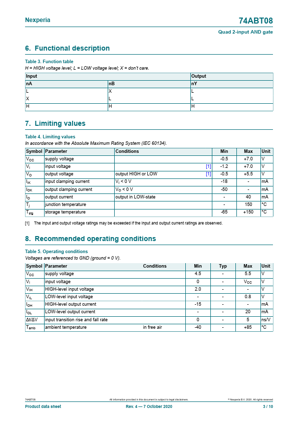
Quad 2-input AND gate The 74ABT08 is a quad 2-input AND gate. This device is fully specified for partial power down applications using IOFF. The IOFF circuitry disables the output, preventing the potentially damaging backflow current through the device when it is powered down. 2. Features and benefits • Supply voltage range from 4.5 V to 5.5 V • BiCMOS high speed and output drive • Direct interface with TTL levels • IOFF circuitry provides partial Power-down mode operation • Latch-up protection exceeds 500 mA per JESD78B class II level A • ESD protection: • HBM JESD22-A114F exceeds 2000 V • MM JESD22-A115-A exceeds 200 V • Specified from -40 °C to +85 °C 3. Ordering information Table 1. Ordering information Ty... |