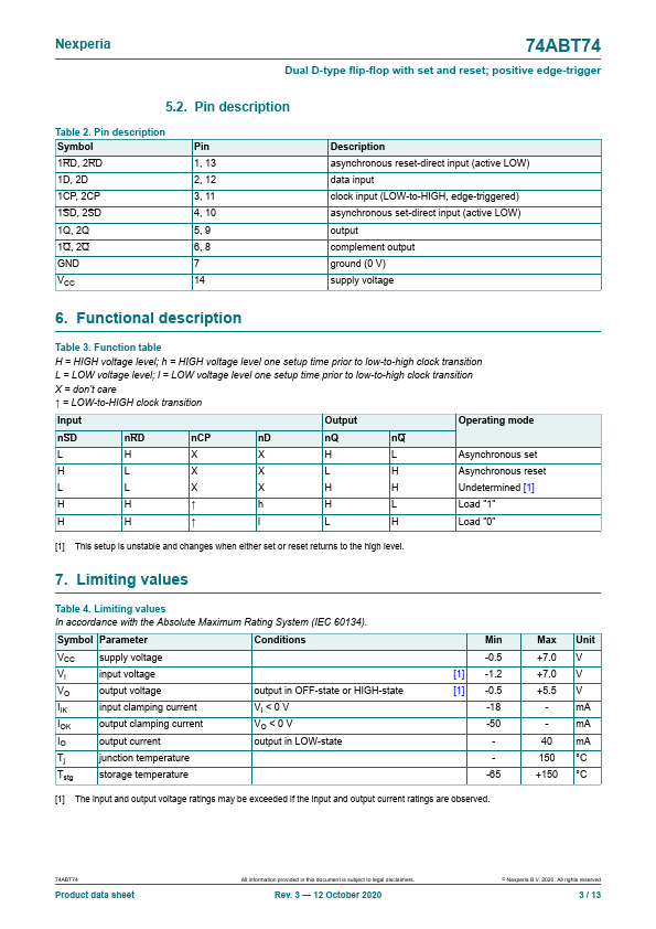
| Description | The 74ABT74 is a dual positive edge triggered D-type flip-flop with individual data (D), clock (CP), set (SD) and reset (RD) inputs, and complementary Q and Q outputs. Data at the D-input that meets the set-up and hold time requirements on the LOW-to-HIGH clock transition will be stored in the flip-... |
| Features |
and benefits
• Supply voltage range from 4.5 V to 5.5 V • BiCMOS high speed and output drive • Direct interface with TTL levels • Power-up 3-state • IOFF circuitry provides partial Power-down mode operation • Latch-up protection exceeds 500 mA per JESD78B class II level A • ESD protection: • HBM JESD22-A114F exceeds 2000 V • MM JESD22-A115-A exceeds 200 V • Specified from -40 °C to +85 °C 3. Ordering information Table 1. Ordering information Type number Package Temperature range Name 74ABT74D -40 °C to +85 °C SO14 74ABT74PW -40 °C to +85 °C TSSOP14 Description plastic small outline pack... |
| Datasheet |
|

| Part Number | Description |
|---|---|
 nexperia |
Dual D-type flip-flop The 74ABT74 is a dual positive edge triggered D-type flip-flop with individual data (D), clock (CP), set (SD) and reset (RD) inputs, and complementary Q and Q outputs. Data at the D-input that meets the set-up and hold time requirements on the LOW-to-HIGH clock transition will be stored in the flip-flop and appear at the Q output. This device is fully specified for partial power down applications using IOFF. The IOFF circuitry disables the output, preventing the potentially damaging backflow current through the device when it is powered down. 2. Features and benefits • Supply voltage range from 4.5 V to 5.5 V • BiCMOS high speed and output drive • Direct interface with TTL levels • Power-up... |
 NXP |
Dual D-type flip-flop The 74ABT74 is a dual positive edge-triggered D-type flip-flop featuring individual data, clock, set, and reset inputs; also true and complementary outputs. Set (SD) and reset (RD) are asynchronous active low inputs and operate independently of the clock input. When set and reset are inactive (high), data at the D input is transferred to the Q and Q outputs on the low-to-high transition of the clock. Data must be stable just one setup time prior to the low-to-high transition of the clock for predictable operation. Clock triggering occurs at a voltage level and is not dir... |
nexperia |
Dual D-type flip-flop The 74ABT74 is a dual positive edge triggered D-type flip-flop with individual data (D), clock (CP), set (SD) and reset (RD) inputs, and complementary Q and Q outputs. Data at the D-input that meets the set-up and hold time requirements on the LOW-to-HIGH clock transition will be stored in the flip-flop and appear at the Q output. This device is fully specified for partial power down applications using IOFF. The IOFF circuitry disables the output, preventing the potentially damaging backflow current through the device when it is powered down. 2. Features and benefits • Supply voltage range from 4.5 V to 5.5 V • BiCMOS high speed and output drive • Direct interface with TTL levels • Power-up... |