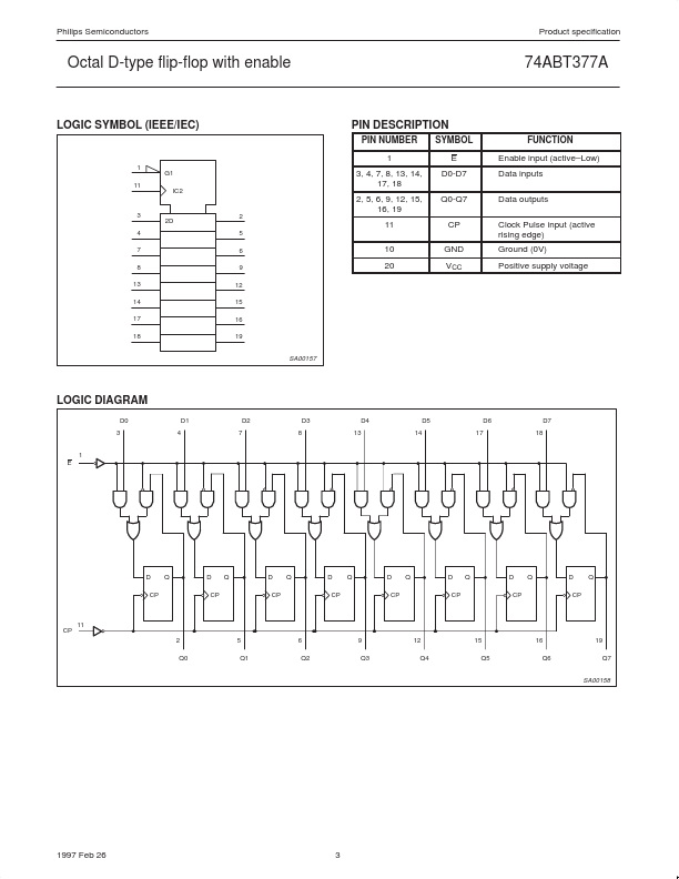
| Description | The 74ABT377A high-performance BiCMOS device combines low static and dynamic power dissipation with high speed and high output drive. The 74ABT377A has 8 edge-triggered D-type flip-flops with individual D inputs and Q outputs. The common buffered clock (CP) input loads all flip-flops simultaneously ... |
| Features |
• Ideal for addressable register applications • 8-bit positive edge-triggered register • Enable for address and data synchronization applications • Output capability: +64mA/-32mA • Latch-up protection exceeds 500mA per Jedec JC40.2 Std 17 • ESD protection exceeds 2000V per MIL STD 883 Method 3015 and 200V per Machine Model DESCRIPTION The 74ABT377A high-performance BiCMOS device combines low static and dynamic power dissipation with high speed and high output drive. The 74ABT377A has 8 edge-triggered D-type flip-flops with individual D inputs and Q outputs. The common buffered clock (CP) inp... |
| Datasheet |
|

| Part Number | Description |
|---|---|
 Fairchild Semiconductor |
Octal Transparent Latch The ABT373 consists of eight latches with 3-STATE outputs for bus organized system applications. The flipflops appear transparent to the data when Latch Enable (LE) is HIGH. When LE is LOW, the data that meets the setup times is latched. Data appears on the bus when the Output Enable (OE) is LOW. When OE is HIGH the bus output is in the high impedance... |
 NXP |
Octal transparent latch The 74ABT373A high-performance BiCMOS device combines low static and dynamic power dissipation with high speed and high output drive. The 74ABT373A device is an octal transparent latch coupled to eight 3-State output buffers. The two sections of the device are controlled independently by Enable (E) and Output Enable (OE) control gates. The data on the D inputs are transferred to the latch outputs when the Latch Enable (E) input is High. The latch remains transparent to the data inputs while E is High, and stores the data that is present one setup time before the High-to-Low enable transition. The 3-State output buffers are designed to drive heavily loaded 3-State buses, MOS memories, or MOS ... |
Fairchild Semiconductor |
Octal D-Type Flip-Flop The ABT374 is an octal D-type flip-flop featuring separate D-type inputs for each flip-flop and 3-STATE outputs for bus-oriented applications. A buffered Clock (CP) and Output Enable (OE) are common to all flip-flops. Ordering Information Order Number 74ABT... |
NXP |
Octal D-type flip-flop The 74ABT374A high-performance BiCMOS device combines low static and dynamic power dissipation with high speed and high output drive. The 74ABT374A is an 8-bit, edge triggered register coupled to eight 3-State output buffers. The two sections of the device are controlled independently by the clock (CP) and Output Enable (OE) control gates. The register is fully edge triggered. The state of each D input, one set-up time before the Low-to-High clock transition, is transferred to the corresponding flip-flop’s Q output. The 3-State output buffers are designed to drive heavily loaded 3-State buses, MOS memories, or MOS microprocessors. The active-Low Output Enable (OE) controls all eight 3-State ... |
Fairchild Semiconductor |
Octal D-Type Flip-Flop The ABT377 has eight edge-triggered, D-type flip-flops with individual D inputs and Q outputs. The common buffered Clock (CP) input loads all flip-flops simultaneously when the Clock Enable (CE) is LOW. The register is fully edge-triggered. The state of each D input, one setup time before the LOW-to-HIGH clock transition, is transferred to the corresponding flip-flop’s Q output. The CE input must be stable only one setup time prior to the LOW-to-HIGH clock transition for predictable operation. Features s Clock enable for address and data synchronization applications s Eight edge-triggered D-type flip-flops s Buffered common clock s See ABT273 for master reset version s See ABT373 for transp... |