| Description | The KA7500C is used for the control circuit of the pulsewidth modulation switching regulator. The KA7500C consists of 5V reference voltage circuit, two error amplifiers, flip flop, an output control circuit, a PWM comparator, a dead-time comparator, and an oscillator. This device can be operated in ... |
| Features |
Internal Regulator Provides a Stable 5V Reference
Supply Trimmed to ±1% Accuracy
Uncommitted Output TR for 200mA Sink or Source
Current
Output Control for Push-Pull or Single-Ended
Operation
Variable Duty Cycle by Dead-Time Control (Pin 4)
Complete PWM Control Circuit
On-Chip Oscillator with Master or Slave Operation Internal Circuit Prohibits Double Pulse at Either
Output
Description
The KA7500C is used for the control circuit of the pulsewidth modulation switching regulator. The KA7500C consists of 5V reference voltage circuit, two error amplifiers, flip flop, an output control ...
|
| Datasheet |
|

| Part Number | Description |
|---|---|
 HUAFUQIN |
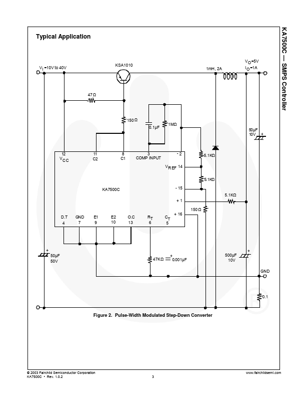
single monolithic chip SHENZHEN HUAFUQIN ELECTRONICS CO.,LTD KA7500 KA7500 KA7500 http://www.hfq123.com 1 REV: A0 2009-12-1 SHENZHEN HUAFUQIN ELECTRONICS CO.,LTD KA7500 http://www.hfq123.com 2 REV: A0 2009-12-1 SHENZHEN HUAFUQIN ELECTRONICS CO.,LTD KA7500 http://www.hfq123.hqew.com 3 REV: A0 2009-12-1 SHENZHEN HUAFUQIN ELECTRONICS CO.,LTD KA7500 http://www.hfq123.com 4 REV: A0 2009-12-1 SHENZHEN HUAFUQIN ELECTRONICS CO.,LTD Typical Application Pulse Width Modulated Step-down Converter VI=10V to 40V KSA1010 47Ω 150Ω 0.1uF 1MΩ 12 Vcc 11 C2 83 C1 COMP INPUT -2 VREF 14 KA7500 - 15 +1 D.T GND E1 E2 O.C 4 7 9 10 13 + 50uF 50V RT CT +16 65 + 47kΩ 0.001uF KA7500 1mH,2A Vo=5V Io=1A ... |
 H&M Semiconductor |
Switching - type pulse width control circuit ... |
 Estek Electronics |
single monolithic chip The KA7500 incorporate on a single monolithic chip all the functions required in the construction of a pulse-width-modulation control circuit. Designed primarily for power supply control ,these devices offer the systems engineer the flexibility to tailor the power supply control circuitry to hos application. The K A7500 contains an error amplifier , anon-chip adjustable oscillator ,a dead- time control comparator ,pulse-steering control flip-flop ,a 5-volt, 1% precision regulator , and output-control circuits. The error amplifier exhibits a common-mode voltage range from -0.3 volts to Vcc -2 volts .The dead time control comparator has a fixed offset that provides approximately 5% deed time ... |
 Samsung |
VOLTAGE-MODE PWM CONTROLLER KA7500B Industrial CD-ROM(Edition 3.0) This Data Sheet is subject to change without notice. Page : 1 ( KA7500B ) (C) 1996 Samsung Electronics Printed in Korea. KA7500B Industrial CD-ROM(Edition 3.0) This Data Sheet is subject to change without notice. Page : 2 ( KA7500B ) (C) 1996 Samsung Electronics Printed in Korea. KA7500B Industrial CD-ROM(Edition 3.0) This Data Sheet is subject to change without notice. Page : 3 ( KA7500B ) (C) 1996 Samsung Electronics Printed in Korea. KA7500B Industrial CD-ROM(Edition 3.0) This Data Sheet is subject to change without notice. Page : 4 ( KA7500B ) (C) 1996 Samsung Electronics Printed in Korea. KA7500B Industrial CD-ROM(Edition 3.0) Thi... |
 Fairchild |
SMPS Controller The KA7500B is used for the control circuit of the PWM switching regulator. The KA7500B consists of 5V reference voltage circuit, two error amplifiers, a flip flop, an output control circuit, a PWM comparator, a dead time comparator and an oscillator. This device can be operated in the switching frequency of 1kHz to 300kHz. 16-DIP 1 16-SOP 1 Internal Block Diagram Rev. 1.0.0 ©2002 Fairchild Semiconductor Corporation KA7500B Absolute Maximum Ratings Parameter Supply Voltage Collector Supply Voltage Output Current Amplifier Input Voltage Power Dissipation (TA = 25°C) Operating Temperature Range Storage Temperature Range Symbol VCC VC IO VIN PD TOPR TSTG Value 42 42 250 VCC +0.3 1 (KA750... |