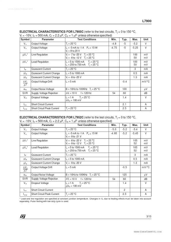
| Description | The L7900 series of three-terminal negative regulators is available in TO-220, ISOWATT220 TO-3 and D2PAK packages and several fixed output voltages, making it useful in a wide range of applications.These regulators can provide local on-card regulation, eliminating the distribution problems associate... |
| Features |
adjustable voltages and currents. SCHEMATIC DIAGRAM
1 2
TO-3
1
3
D2PAK
3 1 2
TO-220
ISOWATT220
November 1999
1/13
www.DataSheet4U.com
L7900
ABSOLUTE MAXIMUM RATINGS
Symbol Vi Io P tot T op T st g Parameter DC Input Voltage (for VO = 5 to 18V) (for V O = 20, 24V) Output Current Power Dissipation Operating Junction Temperature Range Storage Temperature Range Value -35 -40 Internally limited Internally limited 0 to 150 - 65 to 150
o o
Unit V V
C C
THERMAL DATA
Symbol Parameter D PAK 3 62.5
2
TO-220 3 50
ISOWATT220 4 60
TO-3 4 35
Unit
o o
R thj- ca se Thermal Resistance Junction...
|
| Datasheet |
|

| Part Number | Description |
|---|---|
 Inchange Semiconductor |
TO-220C Three Terminal Negative Voltage Regulator INCHANGE Semiconductor isc Product Specification isc Three Terminal Negative Voltage Regulator 7912 FEATURES ·Output current in excess of 1.5A ·Output voltage of -12V ·Internal thermal overload protection ·Output transition Safe-Area compensation ·Minimum Lot-to-Lot variations for robust device performance and reliable operation ABSOLUTE MAXIMUM RATINGS(Ta=25℃) SYMBOL PARAMETER RATING UNIT Vi DC input voltage -35 V Io Output current internally limited Ptot Power dissipation internally limited TOP Operating junction temperature 0~150 ℃ Tstg Storage temperature -55~150 ℃ THERMAL CHARACTERISTICS SYMBOL PARAMETER MAX UNIT Rth j-c Thermal Resistance, Junction to Case 3 ... |
 INCHANGE |
TO-252 Three Terminal Negative Voltage Regulator isc Three Terminal Positive Voltage Regulator FEATURES ·Output current in excess of 1.5A ·Output voltage of -12V ·Internal thermal overload protection ·Output transition Safe-Area compensation ·Minimum Lot-to-Lot variations for robust device performance and reliable operation ABSOLUTE MAXIMUM RATINGS(Ta=25℃) SYMBOL PARAMETER RATING UNIT Vi DC input voltage -35 V Io Output current internally limited Ptot Power dissipation internally limited TOP Operating junction temperature -40~125 ℃ Tstg Storage temperature -55~150 ℃ THERMAL CHARACTERISTICS SYMBOL PARAMETER MAX UNIT Rth j-c Thermal Resistance, Junction to Case 3 ℃/W Rth j-a Thermal Resistance,Junction to Ambi... |