| Description | OptiMOS™ Small-Signal-Transistor Features • N-channel • Enhancement mode • Logic level (4.5V rated) • Avalanche rated • Qualified according to AEC Q101 • 100% lead-free; RoHS compliant; Halogen free BSS119N Product Summary VDS RDS(on),max ID VGS=10 V VGS=4.5 V 100 V 6W 10 0.19 A PG-SOT23 3 1 ... |
| Features |
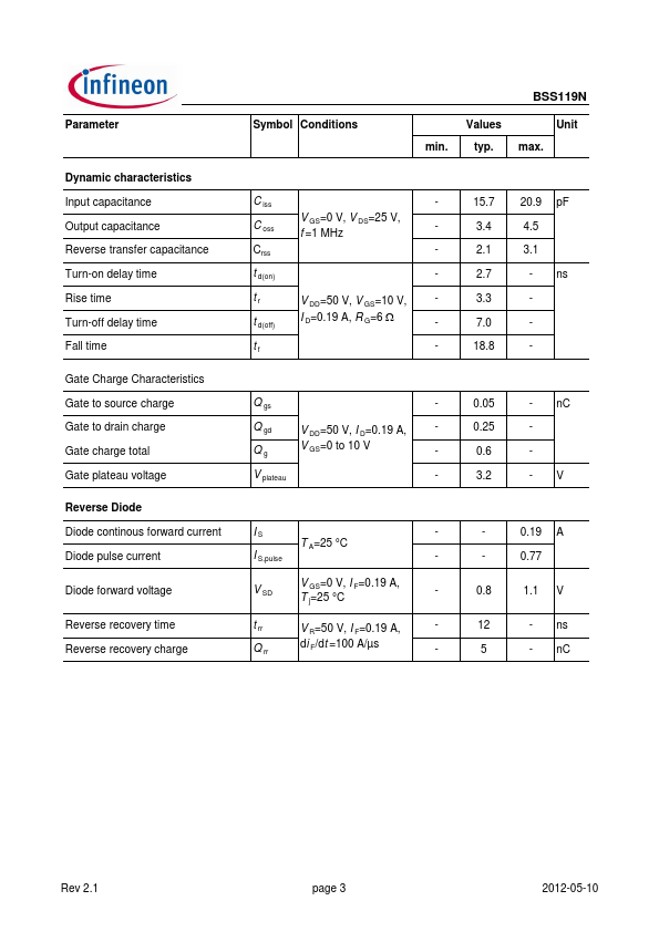
• N-channel • Enhancement mode • Logic level (4.5V rated) • Avalanche rated • Qualified according to AEC Q101 • 100% lead-free; RoHS compliant; Halogen free BSS119N Product Summary VDS RDS(on),max ID VGS=10 V VGS=4.5 V 100 V 6W 10 0.19 A PG-SOT23 3 1 2 Type BSS119N Package SOT23 Tape and Reel Information H6327: 3000 pcs/ reel Maximum ratings, at T j=25 °C, unless otherwise specified Parameter Symbol Conditions Continuous drain current Pulsed drain current ID I D,pulse T A=25 °C T A=70 °C T A=25 °C Marking sSH Halogen free Packing Yes Non dry Value 0.19 0.15 0.77 Unit A Ava... |
| Datasheet |
|

| Part Number | Description |
|---|---|
 Fairchild Semiconductor |
P-Channel Enhancement Mode Field Effect Transistor These P-Channel enhancement mode power field effect transistors are produced using Fairchild's proprietary, high cell density, DMOS technology. This very high density process is designed to minimize on-state resistance, provide rugged and reliable performance and fast switching. They can be used, with a minimum of effort, in most applications requiring up to 0.17A DC and can deliver pulsed currents up to 0.68A. This product is particularly suited to low voltage applications requiring a low current high side switch. Features BSS84: -0.13A, -50V. RDS(ON) = 10Ω @ VGS = -5V. BSS110: -0.17A, -50V. RDS(ON) = 10Ω @ VGS = -10V Voltage controlled p-channel small signal switch. High density cell desi... |
 Siemens Semiconductor |
SIPMOS Small-Signal Transistor BSS 110 SIPMOS ® Small-Signal Transistor • P channel • Enhancement mode • Logic Level • VGS(th) = -0.8...-2.0 V Pin 1 S Type BSS 110 Type BSS 110 BSS 110 BSS 110 Pin 2 G Marking SS 110 Pin 3 D VDS -50 V ID -0.17 A RDS(on) 10 Ω Package TO-92 Ordering Code Q62702-S500 Q62702-S278 Q67000-S568 Tape and Reel Information E6288 E6296 E6325 Maximum Ratings Parameter Drain source voltage Drain-gate voltage Symbol Values -50 -50 Unit V VDS V DGR RGS = 20 kΩ Gate source voltage Continuous drain current VGS ID ± 20 A -0.17 TA = 35 °C DC drain current, pulsed IDpuls -0.68 TA = 25 °C Power dissipation Ptot 0.63 W TA = 25 °C Semiconductor Group 1 12/05/1997 BSS 110 Maximum Ratings ... |
 NXP |
P-channel enhancement mode vertical D-MOS transistor P-channel enhancement mode vertical D-MOS transistor in a TO-92 variant package. handbook, halfpage BSS110 d 1 2 3 g MAM144 s Fig.1 Simplified outline and symbol. PINNING - TO-92 variant PIN 1 2 3 SYMBOL s g d DESCRIPTION source gate drain CAUTION The device is supplied in an antistatic package. The gate-source input must be protected against static discharge during transport or handling. QUICK REFERENCE DATA SYMBOL VDS VGSO VGSth ID RDSon Ptot PARAMETER drain-source voltage (DC) gate-source voltage (DC) gate-source threshold voltage drain current (DC) drain-source on-state resistance total power dissipation ID = −170 mA; VGS = −10 V up to Tamb = 25 °C open drain ID = −1 mA; VDS = VGS... |
 Siemens Semiconductor Group |
SIPMOS Small-Signal Transistor BSS 119 SIPMOS ® Small-Signal Transistor • N channel • Enhancement mode • VGS(th) = 1.6 ...2.6 V Pin 1 G Pin 2 S Pin 3 D Type BSS 119 Type BSS 119 VDS 100 V ID 0.17 A RDS(on) 6Ω Package SOT-23 Marking sSH Ordering Code Q67000-S007 Tape and Reel Information E6327 Maximum Ratings Parameter Drain source voltage Drain-gate voltage Symbol Values 100 100 Unit V VDS VDGR VGS Vgs ID RGS = 20 kΩ Gate source voltage Gate-source peak voltage,aperiodic Continuous drain current ± 14 ± 20 A 0.17 TA = 28 °C DC drain current, pulsed IDpuls 0.68 TA = 25 °C Power dissipation Ptot 0.36 W TA = 25 °C Semiconductor Group 1 Sep-13-1996 BSS 119 Maximum Ratings Parameter Chip or operating ... |
 INFINEON |
SIPMOS Small-Signal Transistor and charts stated herein. Infineon Technologies is an approved CECC manufacturer. BSS119 Information For further information on technology, delivery terms and conditions and prices please contact your nearest Infineon Technologies Office in Germany or our Infineon Technologies Reprensatives worldwide (see address list). Warnings Due to technical requirements components may contain dangerous substances. For information on the types in question please contact your nearest Infineon Technologies Office. Infineon Technologies Components may only be used in life-support devices or systems with the express written approval of Infineon Technologies, if a failure of such components can reasonably ... |