| Description | IRFZ40 IRFZ40FI N - CHANNEL ENHANCEMENT MODE POWER MOS TRANSISTORS TYPE IRFZ40 IRFZ40FI VDSS 50 V 50 V R DS( on) < 0.028 Ω < 0.028 Ω ID 50 A 27 A s TYPICAL RDS(on) = 0.022 Ω s AVALANCHE RUGGED TECHNOLOGY s 100% AVALANCHE TESTED s REPETITIVE AVALANCHE DATA AT 100oC s LOW GATE CHARGE s HIGH CURRE... |
| Features |
e
Tj Max. Operating Junction Temperature
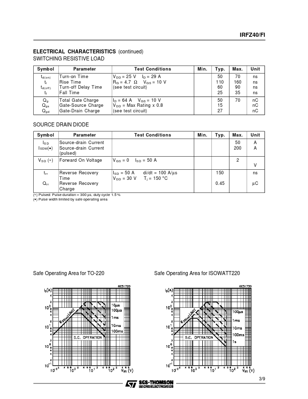
( •) Pulse width limited by safe operating area July 1993 Value IRFZ40 IRFZ40FI 50 50 50 50 ± 20 50 27 35 19 200 200 150 45 1 0.3 2000 -65 to 175 175 Unit V V V A A A W W/oC V oC oC 1/9 IRFZ40/FI THERMAL DATA Rthj-case Rthj- amb R th c-s Tl Thermal Resistance Junction-case Max Thermal Resistance Junction-ambient Max Thermal Resistance Case-sink Typ Maximum Lead Temperature For Soldering Purpose TO-220 1 ISOWATT220 3. 33 6 2. 5 0. 5 300 oC/W oC/W oC/W oC AVALANCHE CHARACTERISTICS Symb ol IA R EAS EAR IA R Pa ra met er Aval... |
| Datasheet |
|

| Part Number | Description |
|---|---|
 Inchange Semiconductor |
N-Channel MOSFET Transistor ·Designed for use in switch mode power supplies and general purpose applications. ABSOLUTE MAXIMUM RATINGS(Ta=25℃) SYMBOL PARAMETER VDSS Drain-Source Voltage VGS Gate-Source Voltage-Continuous ID Drain Current-Continuous IDM Drain Current-Single Pluse PD Total Dissipation @TC=25℃ TJ Max. Operating Junction Temperature Tstg Storage Temperature VALUE UNIT 50 V ±20 V 50 A 200 A 150 W 175 ℃ -65~175 ℃ THERMAL CHARACTERISTICS SYMBOL PARAMETER Rth j-c Rth j-a Thermal Resistance, Junction to Case Thermal Resistance, Junction to Ambient MAX 1.0 62.5 UNIT ℃/W ℃/W isc website:www.iscsemi.cn 1 isc & iscsemi is registered trademark PDF pdfFactory Pro www.fineprint.cn INCHANG... |
 Samsung Electronics |
N-Channel Power MOSFETS ... |
 Motorola Semiconductor |
Power Field Effect Transistors ... |
 STMicroelectronics |
N-Channel Power MOS Transistors T SGS-THOMSON ^ 7 #« [^DWi[L[i(gTOR!]D(gi IRFZ40 IRFZ42 N - CHANNEL ENHANCEMENT MODE POWER MOS TRANSISTORS TYPE IRFZ40 IRFZ42 V Dss 50 V 50 V ^DS(on) 0.028 fi 0.035 n •d 35 A 35 A • VERY LOW Rds (on) • LOW DRIVE ENERGY FOR EASY DRIVE • HIGH TRANSCONDUCTANCE /Crss RATIO INDUSTRIAL APPLICATIONS: • AUTOMOTIVE POWER ACTUATORS • MOTOR CONTROLS • INVERTERS N - channel enhancement mode POWER MOS field effect transistors. Easy drive and very fast switch ing times make these POWER MOS transistors ideal for high speed switching circuits applications such as power actuators driving, motor drive includ ing brushless motor, hydraulic actuators and many other in automotive and automatic guided v... |
 Vishay |
Power MOSFET Third generation power MOSFETs from Vishay provide the designer with the best combination of fast switching, ruggedized device design, low on-resistance and cost-effectiveness. The TO-220AB package is universially preferred for commercial-industrial applications at power dissipation levels to approximately 50 W. The low thermal resistance and low package cost of the TO-220AB contribute to its wide acceptance throughout the industry. ORDERING INFORMATION Package Lead (Pb)-free Lead (Pb)-free and halogen-free TO-220AB IRFZ40PbF IRFZ40PbF-BE3 ABSOLUTE MAXIMUM RATINGS (TC = 25 °C, unless otherwise noted) PARAMETER SYMBOL Drain-source voltage Gate-source voltage Continuous drain current Pul... |
 ART CHIP |
N-CHANNEL POWER MOSFETS IRFZ44/45/40/42 N-CHANNEL POWER MOSFETS FEATURES Lower RDS(ON) Improved inductive ruggedness Fast switching times Rugged polysilicon gate cell structure Lower input capacitance Extended safe operating area Improved high temperature reliability TO-220 IRFZ44/IRFZ45 IRFZ40/IRFZ42 PRODUCT SUMMARY Part Number VDS IRFZ44 60V RDS(on) 0.028Ω ID 35A IRFZ45 60V 0.035Ω 35A IRFZ40 50V 0.028Ω 35A IRFZ42 50V 0.035Ω 35A *Current limited by wire & pin diameter MAXIMUM RATINGS Characteristic Drain-Source Voltage (1) Drain-Gate Voltage (RGS=1 0MΩ) (1) Gate-Source Voltage Continuous Drain Current Tc=25¥ Continuous Drain Current Tc=100¥ Drain Current – Pulsed (3) Gate Current –Pulsed Sin... |
Inchange Semiconductor |
N-Channel MOSFET Transistor ·Designed for use in switch mode power supplies and general purpose applications. ABSOLUTE MAXIMUM RATINGS(Ta=25℃) SYMBOL PARAMETER VDSS Drain-Source Voltage VGS Gate-Source Voltage-Continuous ID Drain Current-Continuous IDM Drain Current-Single Pluse PD Total Dissipation @TC=25℃ TJ Max. Operating Junction Temperature Tstg Storage Temperature VALUE UNIT 50 V ±20 V 27 A 200 A 45 W 175 ℃ -65~175 ℃ THERMAL CHARACTERISTICS SYMBOL PARAMETER Rth j-c Rth j-a Thermal Resistance, Junction to Case Thermal Resistance, Junction to Ambient MAX 3.33 62.5 UNIT ℃/W ℃/W isc website:www.iscsemi.cn 1 isc & iscsemi is registered trademark PDF pdfFactory Pro www.fineprint.cn INCHANG... |