| Description | and charts stated herein. Infineon Technologies is an approved CECC manufacturer. BSS123 Information For further information on technology, delivery terms and conditions and prices please contact your nearest Infineon Technologies Office in Germany or our Infineon Technologies Reprensatives world... |
| Features |
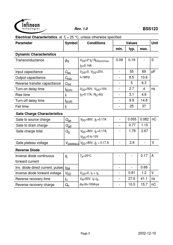
• N-Channel • Enhancement mode • Logic Level • dv/dt rated Product Summary VDS 100 6 0.17 SOT23 V Ω A RDS(on) ID 3 Drain pin 3 Gate pin1 Source pin 2 2 1 VPS05161 Type BSS123 BSS123 Package SOT23 SOT23 Ordering Code Q62702-S512 Q67000-S245 Tape and Reel Information E6327: 3000 pcs/reel E6433: 10000 pcs/reel Marking SAs SAs Maximum Ratings, at Tj = 25 °C, unless otherwise specified Parameter Continuous drain current TA=25°C TA=70°C Symbol ID Value 0.17 0.14 Unit A Pulsed drain current TA=25°C I D puls dv/dt VGS Ptot 0.68 6 ±20 Class 1 0.36 -55... +150 55/150/56 W °C kV/µs V R... |
| Datasheet |
|

| Part Number | Description |
|---|---|
 Siemens Semiconductor Group |
SIPMOS Small-Signal Transistor BSS 100 SIPMOS ® Small-Signal Transistor • N channel • Enhancement mode • Logic Level • VGS(th) = 0.8...2.0V Pin 1 S Type BSS 100 Type BSS 100 BSS 100 BSS 100 Pin 2 G Marking SS 100 Pin 3 D VDS 100 V ID 0.22 A RDS(on) 6Ω Package TO-92 Ordering Code Q62702-S499 Q62702-S007 Q62702-S206 Tape and Reel Information E6288 E6296 E6325 Maximum Ratings Parameter Drain source voltage Drain-gate voltage Symbol Values 100 100 Unit V VDS V DGR RGS = 20 kΩ Gate source voltage Gate-source peak voltage,aperiodic Continuous drain current VGS Vgs ID ± 14 ± 20 A 0.22 TA = 33 °C DC drain current, pulsed IDpuls 0.9 TA = 25 °C Power dissipation Ptot 0.63 W TA = 25 °C Semiconductor Group 1 12... |
 Fairchild Semiconductor |
N-Channel Logic Level Enhancement Mode Field Effect Transistor These N-Channel logic level enhancement mode power field effect transistors are produced using Fairchild's proprietary, high cell density, DMOS technology. This very high density process has been especially tailored to minimize on-state resistance, provide superior switching performance. This product is particularly suited to low voltage, low current applications, such as small servo motor controls, power MOSFET gate drivers, and other switching applications. Features BSS100: 0.22A, 100V. RDS(ON) = 6Ω @ VGS = 10V. BSS123: 0.17A, 100V. RDS(ON) = 6Ω @ VGS = 10V High density cell design for extremely low RDS(ON). Voltage controlled small signal switch. Rugged and reliable. ___________________... |
 Siemens Semiconductor |
SIPMOS Small-Signal Transistor BSS 101 SIPMOS ® Small-Signal Transistor • N channel • Enhancement mode • Logic Level • VGS(th) = 0.8...2.0V Pin 1 S Type BSS 101 Type BSS 101 BSS 101 Pin 2 G Marking SS 101 Pin 3 D VDS 240 V ID 0.13 A RDS(on) 16 Ω Package TO-92 Ordering Code Q62702-S493 Q62702-S636 Tape and Reel Information E6288 E6325 Maximum Ratings Parameter Drain source voltage Drain-gate voltage Symbol Values 240 240 Unit V VDS V DGR RGS = 20 kΩ Gate source voltage Gate-source peak voltage,aperiodic Continuous drain current VGS Vgs ID ± 14 ± 20 A 0.13 TA = 33 °C DC drain current, pulsed IDpuls 0.52 TA = 25 °C Power dissipation Ptot 0.63 W TA = 25 °C Semiconductor Group 1 12/05/1997 BSS 101 M... |
Fairchild Semiconductor |
P-Channel Enhancement Mode Field Effect Transistor These P-Channel enhancement mode power field effect transistors are produced using Fairchild's proprietary, high cell density, DMOS technology. This very high density process is designed to minimize on-state resistance, provide rugged and reliable performance and fast switching. They can be used, with a minimum of effort, in most applications requiring up to 0.17A DC and can deliver pulsed currents up to 0.68A. This product is particularly suited to low voltage applications requiring a low current high side switch. Features BSS84: -0.13A, -50V. RDS(ON) = 10Ω @ VGS = -5V. BSS110: -0.17A, -50V. RDS(ON) = 10Ω @ VGS = -10V Voltage controlled p-channel small signal switch. High density cell desi... |
Siemens Semiconductor |
SIPMOS Small-Signal Transistor BSS 110 SIPMOS ® Small-Signal Transistor • P channel • Enhancement mode • Logic Level • VGS(th) = -0.8...-2.0 V Pin 1 S Type BSS 110 Type BSS 110 BSS 110 BSS 110 Pin 2 G Marking SS 110 Pin 3 D VDS -50 V ID -0.17 A RDS(on) 10 Ω Package TO-92 Ordering Code Q62702-S500 Q62702-S278 Q67000-S568 Tape and Reel Information E6288 E6296 E6325 Maximum Ratings Parameter Drain source voltage Drain-gate voltage Symbol Values -50 -50 Unit V VDS V DGR RGS = 20 kΩ Gate source voltage Continuous drain current VGS ID ± 20 A -0.17 TA = 35 °C DC drain current, pulsed IDpuls -0.68 TA = 25 °C Power dissipation Ptot 0.63 W TA = 25 °C Semiconductor Group 1 12/05/1997 BSS 110 Maximum Ratings ... |
 NXP |
P-channel enhancement mode vertical D-MOS transistor P-channel enhancement mode vertical D-MOS transistor in a TO-92 variant package. handbook, halfpage BSS110 d 1 2 3 g MAM144 s Fig.1 Simplified outline and symbol. PINNING - TO-92 variant PIN 1 2 3 SYMBOL s g d DESCRIPTION source gate drain CAUTION The device is supplied in an antistatic package. The gate-source input must be protected against static discharge during transport or handling. QUICK REFERENCE DATA SYMBOL VDS VGSO VGSth ID RDSon Ptot PARAMETER drain-source voltage (DC) gate-source voltage (DC) gate-source threshold voltage drain current (DC) drain-source on-state resistance total power dissipation ID = −170 mA; VGS = −10 V up to Tamb = 25 °C open drain ID = −1 mA; VDS = VGS... |
Siemens Semiconductor Group |
SIPMOS Small-Signal Transistor BSS 119 SIPMOS ® Small-Signal Transistor • N channel • Enhancement mode • VGS(th) = 1.6 ...2.6 V Pin 1 G Pin 2 S Pin 3 D Type BSS 119 Type BSS 119 VDS 100 V ID 0.17 A RDS(on) 6Ω Package SOT-23 Marking sSH Ordering Code Q67000-S007 Tape and Reel Information E6327 Maximum Ratings Parameter Drain source voltage Drain-gate voltage Symbol Values 100 100 Unit V VDS VDGR VGS Vgs ID RGS = 20 kΩ Gate source voltage Gate-source peak voltage,aperiodic Continuous drain current ± 14 ± 20 A 0.17 TA = 28 °C DC drain current, pulsed IDpuls 0.68 TA = 25 °C Power dissipation Ptot 0.36 W TA = 25 °C Semiconductor Group 1 Sep-13-1996 BSS 119 Maximum Ratings Parameter Chip or operating ... |
 INFINEON |
SIPMOS Small-Signal Transistor and charts stated herein. Infineon Technologies is an approved CECC manufacturer. BSS119 Information For further information on technology, delivery terms and conditions and prices please contact your nearest Infineon Technologies Office in Germany or our Infineon Technologies Reprensatives worldwide (see address list). Warnings Due to technical requirements components may contain dangerous substances. For information on the types in question please contact your nearest Infineon Technologies Office. Infineon Technologies Components may only be used in life-support devices or systems with the express written approval of Infineon Technologies, if a failure of such components can reasonably ... |
 Infineon Technologies |
Small-Signal-Transistor OptiMOS™ Small-Signal-Transistor Features • N-channel • Enhancement mode • Logic level (4.5V rated) • Avalanche rated • Qualified according to AEC Q101 • 100% lead-free; RoHS compliant; Halogen free BSS119N Product Summary VDS RDS(on),max ID VGS=10 V VGS=4.5 V 100 V 6W 10 0.19 A PG-SOT23 3 1 2 Type BSS119N Package SOT23 Tape and Reel Information H6327: 3000 pcs/ reel Maximum ratings, at T j=25 °C, unless otherwise specified Parameter Symbol Conditions Continuous drain current Pulsed drain current ID I D,pulse T A=25 °C T A=70 °C T A=25 °C Marking sSH Halogen free Packing Yes Non dry Value 0.19 0.15 0.77 Unit A Avalanche energy, single pulse E AS I D=0.19 A, R GS=25 W 2... |
 JCET |
N-Channel MOSFET JIANGSU CHANGJIANG ELECTRONICS TECHNOLOGY CO., LTD SOT-23 Plastic-Encapsulate MOSFETS BSS123 N Channel MOSFET V(BR)DSS 100 V RDS(on)MAX 6Ω@10V 10Ω@4.5V ID 0.17A FEATURE Surface Mount Package High Density Cell Design for Extremely Low RDS(ON) Voltage Controlled Small Signal Switch Rugged and Reliable SOT-23 1. GATE 2. SOURCE 3. DRAIN APPLICATION Small Servo Motor Controls Power MOSFET Gate Drivers Switching Application MARKING Equivalent Circuit ABSOLUTE MAXIMUM RATINGS (Ta=25℃ unless otherwise noted) Parameter N-MOSFET Drain-Source Voltage Gate-Source Voltage Continuous Drain Current (note 1) Pulsed Drain Current (tp=10us) Continous Source-Drain Diode Current Powe... |
NXP |
N-channel transistor Logic level FET N-channel enhancement mode field-effect transistor in a plastic envelope using ’trench’ technology. Applications:• Relay driver • High-speed line driver • Telephone ringer The BSS123 is supplied in the SOT23 subminiature surface mounting package. PINNING PIN DESCRIPTION 1 gate 2 source 3 drain SOT23 3 Top view 12 LIMITING VALUES Limiting values in accordance with the Absolute Maximum System (IEC 134) SYMBOL PARAMETER CONDITIONS VDSS VDGR VGS ID IDM PD Tj, Tstg Drain-source voltage Drain-gate voltage Gate-source voltage Continuous drain current Pulsed drain current Total power dissipation Operating junction and storage temperature Tj = 25 ˚C to 150˚C Tj = 25 ˚C to 150˚C; RGS... |
 Diodes Incorporated |
N-Channel MOSFET and Applications These N-Channel enhancement mode field effect transistors are produced using Diodes Incorporated’s proprietary, high density and advanced trench technology. These products have been designed to minimize on-state resistance while providing rugged, reliable and fast switching performance. These products are particularly suited for lowvoltage, low-current applications such as: • Small servo motor controls • Power MOSFET gate drivers • Switching applications Features and Benefits • Low Gate Threshold Voltage • Low Input Capacitance • Fast Switching Speed • Low Input/Output Leakage • High Drain-Source Voltage Rating • Totally Lead-Free & Fully RoHS Compliant (Notes 1 & 2) • Halo... |
Fairchild Semiconductor |
N-Channel Logic Level Enhancement Mode Field Effect Transistor These N-Channel enhancement mode field effect transistors are produced using Fairchild’s proprietary, high cell density, DMOS technology. These products have been designed to minimize on-state resistance while provide rugged, reliable, and fast switching performance.These products are particularly suited for low voltage, low current applications such as small servo motor control, power MOSFET gate drivers, and other switching applications. Features • 0.17 A, 100 V. RDS(ON) = 6Ω @ VGS = 10 V RDS(ON) = 10Ω @ VGS = 4.5 V • High density cell design for extremely low RDS(ON) • Rugged and Reliable • Compact industry standard SOT-23 surface mount package DD SOT-23 S G Absolute Maximum Ratings ... |
 UTC |
N-CHANNEL POWER MOSFET The UTC BSS123 is an N-channel mode Power MOSFET, it uses UTC’s advanced technology to provide the customers with low CRSS. The UTC BSS123 is suitable for Automotive and Other Applications Requiring. FEATURES * RDS(on) ≤ 6.0Ω @ VGS=10V, ID=100mA * Low CRSS SYMBOL Power MOSFET ORDERING INFORMATION Ordering Number Lead Free Halogen Free Package BSS123L-AE3-R BSS123G-AE3-R SOT-23 Note: Pin Assignment: G: Gate S: Source D: Drain Pin Assignment 123 GSD Packing Tape Reel MARKING www.unisonic.com.tw Copyright © 2018 Unisonic Technologies Co., Ltd 1 of 3 QW-R209-133.b BSS123 Preliminary Power MOSFET ABSOLUTE MAXIMUM RATINGS PARAMETER SYMBOL RATINGS UNIT Drain-Source... |
 PAN JIT |
100V N-Channel Enhancement Mode MOSFE PBSS123 100V N-Channel Enhancement Mode MOSFET – ESD Protected Voltage 100 V Current 170 mA SOT-23 Features RDS(ON) , VGS@10V, ID@170mA<6Ω RDS(ON) , [email protected], ID@130mA<10Ω Advanced Trench Process Technology Specially Designed for Switch Load, PWM Application, etc ESD Protected 2KV HBM Lead free in compliance with EU RoHS 2011/65/EU directive Green molding compound as per IEC61249 Std.. (Halogen Free) Mechanical Data Case: SOT-23 Package Terminals: Solderable per MIL-STD-750, Method 2026 TOP VIEW Unit: inch(mm) FIG.183 Maximum Ratings and Thermal Characteristics o (TA=25 C unless otherwise noted) PARAMETER Drain-Source Voltage Gate-Source Voltage Continuo... |
 LITE-ON |
N-Channel 100V MOSFET N-Channel 100V MOSFET Features: Surface-mounted package Halogen free Application DC-DC Portable appliance Power management BSS123 BVDSS= 100V , ΩRDS(ON)< 6 @VGS= 10V ID= 0.17A Absolute Maximum Ratings (TA=25℃Unless Otherwise Noted) Parameter Symbol Marking Drain-Source Voltage VDSS Gate-Source Voltage Continuous Drain Current(1) ℃Ta=25 Pulsed Drain Current(2) Power Dissipation(FR-5 board)(3) ℃Ta=25 Operating Junction and Storage Temperature Range VGS ID IDM PD TJ, Tstg BSS123 SA 100 ±20 0.17 0.68 225 -55 to150 Thermal Characteristics Symbol Characteristic RθJA :Note Junction-to-Ambient (1) The Power dissipation of the package may result in a lower continuous drain current.... |