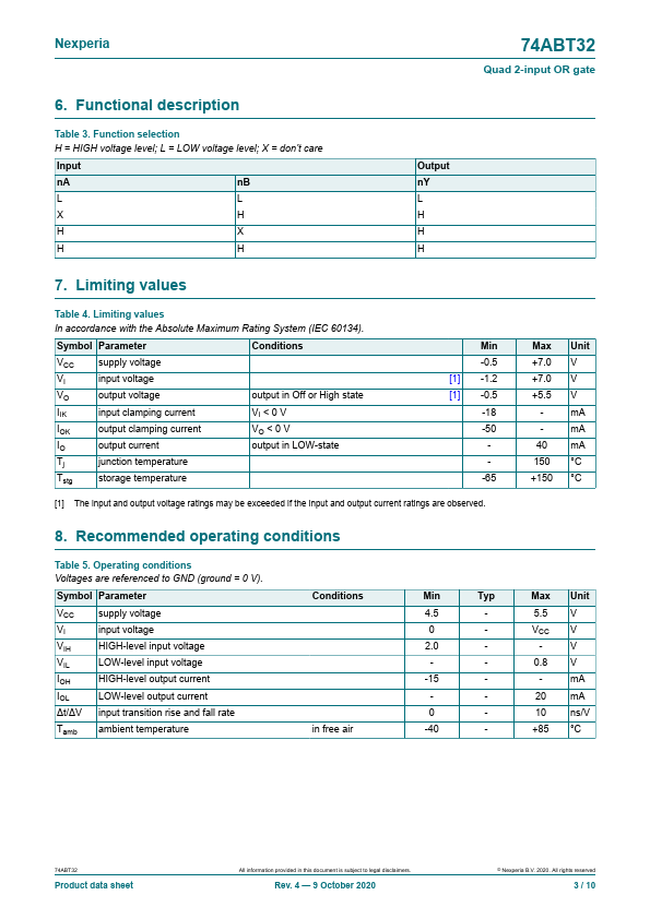
| Description | The 74ABT32 is a quad 2-input OR gate. This device is fully specified for partial power down applications using IOFF. The IOFF circuitry disables the output, preventing the potentially damaging backflow current through the device when it is powered down. 2. Features and benefits • Supply voltage ra... |
| Features |
and benefits
• Supply voltage range from 4.5 V to 5.5 V • BiCMOS high speed and output drive • Direct interface with TTL levels • IOFF circuitry provides partial Power-down mode operation • Latch-up protection exceeds 500 mA per JESD78B class II level A • ESD protection: • HBM JESD22-A114F exceeds 2000 V • MM JESD22-A115-A exceeds 200 V • Specified from -40 °C to +85 °C 3. Ordering information Table 1. Ordering information Type number Package Temperature range Name 74ABT32D -40 °C to +85 °C SO14 74ABT32PW -40 °C to +85 °C TSSOP14 Description plastic small outline package; 14 leads; body... |
| Datasheet |
|

| Part Number | Description |
|---|---|
 NXP |
Quad 2-input OR gate PIN NUMBER 1, 2, 4, 5, 9, 10, 12, 13 3, 6, 8, 11 7 14 SYMBOL An, Bn Yn GND VCC NAME AND FUNCTION Data inputs Data outputs Ground (0V) Positive supply voltage SF00041 FUNCTION TABLE INPUTS An L L H Bn L H L OUTPUT Yn L H H H LOGIC SYMBOL 1 2 4 5 9 10 12 13 H H NOTES: H = High voltage level L = Low voltage level A0 B0 A1 B1 A2 B2 A3 B3 Y0 Y1 Y2 Y3 VCC = Pin 14 GND = Pin 7 3 6 8 11 SA00355 ORDERING INFORMATION PACKAGES 14-Pin Plastic DIP 14-Pin plastic SO 14-Pin Plastic SSOP Type II 14-Pin Plastic TSSOP Type I TEMPERATURE RANGE –40°C to +85°C –40°C to +85°C –40°C to +85°C –40°C to +85°C OUTSIDE NORTH AMERICA 74ABT32 N 74ABT32 D 74ABT32 DB 74ABT32 PW NORTH AMERICA 74ABT32 N 74ABT32 D... |
 nexperia |
Quad 2-input OR gate The 74ABT32 is a quad 2-input OR gate. This device is fully specified for partial power down applications using IOFF. The IOFF circuitry disables the output, preventing the potentially damaging backflow current through the device when it is powered down. 2. Features and benefits • Supply voltage range from 4.5 V to 5.5 V • BiCMOS high speed and output drive • Direct interface with TTL levels • IOFF circuitry provides partial Power-down mode operation • Latch-up protection exceeds 500 mA per JESD78B class II level A • ESD protection: • HBM JESD22-A114F exceeds 2000 V • MM JESD22-A115-A exceeds 200 V • Specified from -40 °C to +85 °C 3. Ordering information Table 1. Ordering information Typ... |
nexperia |
Quad 2-input OR gate The 74ABT32 is a quad 2-input OR gate. This device is fully specified for partial power down applications using IOFF. The IOFF circuitry disables the output, preventing the potentially damaging backflow current through the device when it is powered down. 2. Features and benefits • Supply voltage range from 4.5 V to 5.5 V • BiCMOS high speed and output drive • Direct interface with TTL levels • IOFF circuitry provides partial Power-down mode operation • Latch-up protection exceeds 500 mA per JESD78B class II level A • ESD protection: • HBM JESD22-A114F exceeds 2000 V • MM JESD22-A115-A exceeds 200 V • Specified from -40 °C to +85 °C 3. Ordering information Table 1. Ordering information Typ... |
 Fairchild Semiconductor |
Octal Transparent Latch The ABT373 consists of eight latches with 3-STATE outputs for bus organized system applications. The flipflops appear transparent to the data when Latch Enable (LE) is HIGH. When LE is LOW, the data that meets the setup times is latched. Data appears on the bus when the Output Enable (OE) is LOW. When OE is HIGH the bus output is in the high impedance... |
NXP |
Octal transparent latch The 74ABT373A high-performance BiCMOS device combines low static and dynamic power dissipation with high speed and high output drive. The 74ABT373A device is an octal transparent latch coupled to eight 3-State output buffers. The two sections of the device are controlled independently by Enable (E) and Output Enable (OE) control gates. The data on the D inputs are transferred to the latch outputs when the Latch Enable (E) input is High. The latch remains transparent to the data inputs while E is High, and stores the data that is present one setup time before the High-to-Low enable transition. The 3-State output buffers are designed to drive heavily loaded 3-State buses, MOS memories, or MOS ... |
Fairchild Semiconductor |
Octal D-Type Flip-Flop The ABT374 is an octal D-type flip-flop featuring separate D-type inputs for each flip-flop and 3-STATE outputs for bus-oriented applications. A buffered Clock (CP) and Output Enable (OE) are common to all flip-flops. Ordering Information Order Number 74ABT... |
NXP |
Octal D-type flip-flop The 74ABT374A high-performance BiCMOS device combines low static and dynamic power dissipation with high speed and high output drive. The 74ABT374A is an 8-bit, edge triggered register coupled to eight 3-State output buffers. The two sections of the device are controlled independently by the clock (CP) and Output Enable (OE) control gates. The register is fully edge triggered. The state of each D input, one set-up time before the Low-to-High clock transition, is transferred to the corresponding flip-flop’s Q output. The 3-State output buffers are designed to drive heavily loaded 3-State buses, MOS memories, or MOS microprocessors. The active-Low Output Enable (OE) controls all eight 3-State ... |
Fairchild Semiconductor |
Octal D-Type Flip-Flop The ABT377 has eight edge-triggered, D-type flip-flops with individual D inputs and Q outputs. The common buffered Clock (CP) input loads all flip-flops simultaneously when the Clock Enable (CE) is LOW. The register is fully edge-triggered. The state of each D input, one setup time before the LOW-to-HIGH clock transition, is transferred to the corresponding flip-flop’s Q output. The CE input must be stable only one setup time prior to the LOW-to-HIGH clock transition for predictable operation. Features s Clock enable for address and data synchronization applications s Eight edge-triggered D-type flip-flops s Buffered common clock s See ABT273 for master reset version s See ABT373 for transp... |
NXP |
Octal D-type flip-flop The 74ABT377A high-performance BiCMOS device combines low static and dynamic power dissipation with high speed and high output drive. The 74ABT377A has 8 edge-triggered D-type flip-flops with individual D inputs and Q outputs. The common buffered clock (CP) input loads all flip-flops simultaneously when the Enable (E) input is Low. The register is fully edge triggered. The state of each D input, one set-up time before the Low-to-High clock transition, is transferred to the corresponding flip-flop’s Q output. The E input must be stable one setup time prior to the Low-to-High clock transition for predictable operation. • Power-up reset QUICK REFERENCE DATA SYMBOL tPLH tPHL CIN ICCH PARAMETER... |