| Description | BSP 92 SIPMOS ® Small-Signal Transistor • P channel • Enhancement mode • Logic Level • VGS(th) = -0.8...-2.0 V Pin 1 G Type BSP 92 Type BSP 92 Pin 2 D Pin 3 S Pin 4 D VDS -240 V ID -0.2 A RDS(on) 20 Ω Package SOT-223 Marking BSP 92 Ordering Code Q62702-S653 Tape and Reel Information E6327 ... |
| Features |
g RthJA RthJS
1) Transistor on epoxy pcb 40 mm x 40 mm x 1,5 mm with 6 cm2 copper area for drain connection
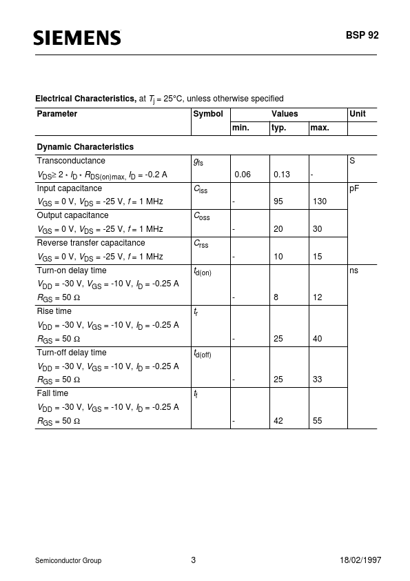
Electrical Characteristics, at Tj = 25°C, unless otherwise specified Parameter Symbol min. Static Characteristics Drain- source breakdown voltage Values typ. max. Unit
V(BR)DSS
-240 -1.5 -0.1 -10 -10 12 -2
V
VGS = 0 V, ID = -0.25 mA, Tj = 25 °C
Gate threshold voltage
VGS(th)
-0.8
VGS=VDS, ID = -1 mA
Zero gate voltage drain current
IDSS
-1 -100 -0.2
µA
VDS = -240 V, VGS = 0 V, Tj = 25 °C VDS = -240 V, VGS = 0 V, Tj = 125 °C VDS = -60 V, VGS = 0 V, Tj = 25 °C
Gate-source leakage ...
|
| Datasheet |
|

| Part Number | Description |
|---|---|
 NXP |
N-Channel MOSFET N-channel enhancement mode field-effect transistor in a plastic package using TrenchMOS™1 technology. Product availability: BSP030 in SOT223. 2. Features s TrenchMOS™ technology s Fast switching s Low on-state resistance s Logic level compatible s Surface mount package. 3. Applications s Motor and actuator driver c c s Battery management s High speed, low resistance switch. 4. Pinning information Table 1: Pinning - SOT223, simplified outline and symbol Pin Description Simplified outline 1 gate (g) 2 drain (d) 4 3 source (s) 4 drain (d) 03ab45 1 23 SOT223 Symbol d g 03ab30 s N-channel MOSFET 1. TrenchMOS is a trademark of Royal Philips Electronics. Philips Semiconductors BSP030... |
NXP |
P-channel enhancement mode vertical D-MOS transistor 4 d DESCRIPTION P-channel enhancement mode vertical D-MOS transistor in a 4-pin plastic SOT223 SMD package. g CAUTION The device is supplied in an antistatic package. The gate-source input must be protected against static discharge during transport or handling. s 1 Top view 2 3 MAM121 Fig.1 Simplified outline and symbol. QUICK REFERENCE DATA SYMBOL VDS VSD VGS VGSth ID RDSon Ptot PARAMETER drain-source voltage (DC) source-drain diode forward voltage gate-source voltage (DC) gate-source threshold voltage drain current (DC) drain-source on-state resistance total power dissipation ID = −1 mA; VDS = VGS Ts = 100 °C Ts = 100 °C IS = −1.25 A CONDITIONS − − − −1 − − MIN. MAX. −30 −1.3 ±20 −2.... |
NXP |
N-channel enhancement mode TrenchMOS transistor N-channel enhancement mode field-effect transistor in a plastic envelope using ’trench’ technology. Applications:• Motor and relay drivers • d.c. to d.c. converters • Logic level translator The BSP100 is supplied in the SOT223 surface mounting package. PINNING PIN 1 2 3 4 gate drain source drain (tab) DESCRIPTION SOT223 4 1 2 3 LIMITING VALUES Limiting values in accordance with the Absolute Maximum System (IEC 134) SYMBOL PARAMETER VDSS VDGR VGS ID IDM PD Tj, Tstg Drain-source voltage Drain-gate voltage Gate-source voltage Continuous drain current Pulsed drain current Total power dissipation Operating junction and storage temperature CONDITIONS Tj = 25 ˚C to 150˚C Tj = 25 ˚C to 150˚C; ... |
NXP |
N-channel enhancement mode vertical D-MOS transistor N-channel enhancement mode vertical D-MOS transistor in a miniature SOT223 envelope and intended for use in relay, high-speed and line transformer drivers. PINNING - SOT223 PIN 1 2 3 4 gate drain source drain 1 Top view 2 3 MAM054 BSP106 QUICK REFERENCE DATA SYMBOL VDS ID RDS(on) VGS(th) PARAMETER drain-source voltage drain current drain-source on-resistance gate-source threshold voltage CONDITIONS − DC value ID = 200 mA VGS = 10 V ID = 1 mA VGS = VDS MAX. 60 425 4 3 UNIT V mA Ω V PIN CONFIGURATION handbook, halfpage 4 d DESCRIPTION g s Fig.1 Simplified outline and symbol. April 1995 2 Philips Semiconductors Product specification N-channel enhancement mode vertical D-MOS transis... |
NXP |
N-channel enhancement mode vertical D-MOS transistor N-channel enhancement mode vertical D-MOS transistor in a miniature SOT223 envelope. Intended for use as a line current interruptor in telephone sets and for applications in relay, high-speed and line transformer driver switching. PINNING - SOT223 PIN 1 2 3 4 gate drain source drain Fig.1 Simplified outline and symbol. DESCRIPTION 1 Top view 2 3 MAM054 BSP107 QUICK REFERENCE DATA SYMBOL VDS VGS(th) ID RDS(on) PARAMETER drain-source voltage (DC) gate-source threshold voltage drain current (DC) drain-source on-state resistance MAX. 200 2.4 200 28 V V mA Ω UNIT handbook, halfpage 4 d g s April 1995 2 Philips Semiconductors Product specification N-channel enhancement mode vertical D-M... |
NXP |
N-channel enhancement mode vertical D-MOS transistor N-channel enhancement mode vertical D-MOS transistor in a miniature SOT223 envelope and intended for use in relay, high-speed and line-transformer drivers. FEATURES • Direct interface to C-MOS, TTL, etc. • High-speed switching • No secondary breakdown PINNING - SOT223 1 2 3 4 = gate = drain = source = drain ID = 500 mA; VGS = 10 V Transfer admittance ID = 500 mA; VDS = 15 V Yfs RDS(on) QUICK REFERENCE DATA Drain-source voltage Gate-source voltage (open drain) Drain current (DC) Total power dissipation up to Tamb = 25 °C Drain-source ON-resistance VDS ± VGSO ID Ptot BSP108 max. max. max. max. typ. max. 80 V 20 V 500 mA 1.5 W 2.0 Ω 3.0 Ω min. typ. 150 mS 300 mS Marking code BSP108 P... |
NXP |
N-channel enhancement mode vertical D-MOS transistor N-channel enhancement mode vertical D-MOS transistor in a miniature SOT223 envelope and designed for use in telephone ringer circuits and for application in relay, high-speed and line transformer drivers. FEATURES • Direct interface to C-MOS, TTL, etc. • High-speed switching • No secondary breakdown PINNING - SOT223 1 = gate 2 = drain 3 = source 4 = drain MARKING CODE BSP110 PIN CONFIGURATION QUICK REFERENCE DATA Drain-source voltage Drain source voltage (non-repetitive peak; tp ≤ 2 ms) Gate-source voltage (open drain) Drain current (DC) Total power dissipation up to Tamb = 25 °C Drain-source ON-resistance ID = 200 mA; VGS = 10 V Transfer admittance ID = 200 mA; VDS = 15 V Yfs min. typ. ... |
NXP |
N-channel enhancement mode vertical D-MOS transistor N-channel enhancement mode vertical D-MOS transistor in a miniature SOT223 envelope and designed for use as a line current interrupter in telephone sets and for application in relay, high-speed and line-transformer drivers. FEATURES • Direct interface to C-MOS, TTL, etc. • High-speed switching • No secondary breakdown QUICK REFERENCE DATA Drain-source voltage Drain-current (DC) Drain-source ON-resistance ID = 250 mA; VGS = 10 V Gate threshold voltage PINNING - SOT223 1 = gate 2 = drain 3 = source 4 = drain Marking code BSP120 PIN CONFIGURATION RDS(on) VGS(th) typ. max. max. VDS ID max. max. BSP120 200 V 250 mA 7 Ω 12 Ω 2.8 V handbook, halfpage 4 d g 1 Top view 2 3 MAM054 s Fig.1 S... |
NXP |
N-channel enhancement mode vertical D-MOS transistor N-channel enhancement mode vertical D-MOS transistor in a miniature SOT223 envelope and designed for use as a line current interrupter in telephone sets and for application in relay, high-speed and line-transformer drivers. FEATURES • Direct interface to C-MOS, TTL, etc. • High-speed switching • No secondary breakdown PINNING - SOT223 1 = gate 2 = drain 3 = source 4 = drain Marking code BSP121 Transfer admittance ID = 400 mA; VDS = 25 V Yfs min. typ. QUICK REFERENCE DATA Drain source voltage Gate-source voltage (open drain) Drain current (DC) Total power dissipation up to Tamb = 25 °C Drain-source on-resistance ID = 400 mA; VGS = 10 V RDS(on) typ. max. Ptot max. VDS ±VGSO ID max. max. ma... |
NXP |
N-channel enhancement mode vertical D-MOS transistor N-channel enhancement mode vertical D-MOS transistor in a SOT223 envelope and intended for use as a line current interruptor in telephone sets and for applications in relay, high-speed and line transformer drivers. PINNING - SOT223 PIN 1 2 3 4 gate drain source drain Fig.1 Simplified outline (SOT223) and symbol. DESCRIPTION QUICK REFERENCE DATA SYMBOL VDS ID RDS(on) VGS(th) PARAMETER drain-source voltage DC drain current drain-source on-resistance gate-source threshold voltage BSP122 MAX. 200 550 2.5 2 V UNIT mA Ω V handbook, halfpage 4 d g 1 Top view 2 3 MAM054 s LIMITING VALUES In accordance with the Absolute Maximum System (IEC 134). SYMBOL VDS ±VGSO ID IDM Ptot Tstg Tj PARAME... |
 Siemens Semiconductor Group |
SIPMOS Small-Signal Transistor (N channel Enhancement mode Logic Level) BSP 123 SIPMOS ® Small-Signal Transistor • N channel • Enhancement mode • Logic Level • VGS(th) = 0.8...2.0V Pin 1 G Type BSP 123 Type BSP 123 Pin 2 D Pin 3 S Pin 4 D VDS 100 V ID 0.38 A RDS(on) 6Ω Package SOT-223 Marking BSP 123 Ordering Code Q67000-S306 Tape and Reel Information E6327 Maximum Ratings Parameter Drain source voltage Drain-gate voltage Symbol Values 100 100 Unit V VDS VDGR VGS Vgs ID RGS = 20 kΩ Gate source voltage Gate-source peak voltage,aperiodic Continuous drain current ± 14 ± 20 A 0.38 TA = 29 °C DC drain current, pulsed IDpuls 0.68 TA = 25 °C Power dissipation Ptot 1.7 W TA = 25 °C Semiconductor Group 1 Sep-12-1996 BSP 123 Maximum Ratings Paramet... |
 Infineon Technologies AG |
SIPMOS Small-Signal-Transistor and charts stated herein. Infineon Technologies is an approved CECC manufacturer. BSP123 Information For further information on technology, delivery terms and conditions and prices please contact your nearest Infineon Technologies Office in Germany or our Infineon Technologies Reprensatives worldwide (see address list). Warnings Due to technical requirements components may contain dangerous substances. For information on the types in question please contact your nearest Infineon Technologies Office. Infineon Technologies Components may only be used in life-support devices or systems with the express written approval of Infineon Technologies, if a failure of such components can reasonably ... |
Siemens Semiconductor Group |
SIPMOS Small-Signal Transistor (N channel Enhancement mode) BSP 125 SIPMOS ® Small-Signal Transistor • N channel • Enhancement mode • VGS(th) = 1.5 ...2.5 V Pin 1 G Type BSP 125 Type BSP 125 BSP 125 Pin 2 D Pin 3 S Pin 4 D VDS 600 V ID 0.12 A RDS(on) 45 Ω Package SOT-223 Marking BSP 125 Ordering Code Q62702-S654 Q67000-S284 Tape and Reel Information E6327 E6433 Maximum Ratings Parameter Drain source voltage Drain-gate voltage Symbol Values 600 600 Unit V VDS VDGR VGS Vgs ID RGS = 20 kΩ Gate source voltage Gate-source peak voltage,aperiodic Continuous drain current ± 14 ± 20 A 0.12 TA = 39 °C DC drain current, pulsed IDpuls 0.48 TA = 25 °C Power dissipation Ptot 1.7 W TA = 25 °C Semiconductor Group 1 Sep-12-1996 BSP 125 Maxi... |
Infineon Technologies AG |
SIPMOS Power-Transistor and charts stated herein. Infineon Technologies is an approved CECC manufacturer. BSP125 Information For further information on technology, delivery terms and conditions and prices please contact your nearest Infineon Technologies Office in Germany or our Infineon Technologies Reprensatives worldwide (see address list). Warnings Due to technical requirements components may contain dangerous substances. For information on the types in question please contact your nearest Infineon Technologies Office. Infineon Technologies Components may only be used in life-support devices or systems with the express written approval of Infineon Technologies, if a failure of such components can reasonably ... |
NXP |
N-channel enhancement mode vertical D-MOS transistor N-channel enhancement mode vertical D-MOS transistor in a miniature SOT223 envelope and designed for use as a line interrupter in telephone sets and for application in relay, high-speed and line-transformer drivers. FEATURES • Direct interface to C-MOS, TTL, etc. • High-speed switching. • No secondary breakdown. PINNING - SOT223 1 = gate 2 = drain 3 = source 4 = drain Marking code BSP126 QUICK REFERENCE DATA Drain-source voltage Drain current (DC) Total power dissipation up to Tamb = 25 °C Drain-source on-resistance ID = 300 mA; VGS = 10 V Gate-source threshold voltage RDS(on) VGS(th) VDS ID Ptot BSP126 max. max. max. typ. max. max. 250 V 350 mA 1.5 W 5.0 Ω 7.0 Ω 2 V PIN CONFIGURATION h... |
NXP |
N-channel enhancement mode vertical D-MOS transistor N-channel enhancement mode vertical D-MOS transistor in a SOT223 envelope and intended for use as a line current interruptor in telephone sets and for applications in relay, high-speed and line transformer drivers. PINNING - SOT223 1 2 3 MAM054 BSP127 QUICK REFERENCE DATA SYMBOL VDS ID RDS(on) VGS(th) PARAMETER drain-source voltage DC drain current drain-source on-resistance gate-source threshold voltage MAX. 270 350 8 2 V mA Ω V UNIT handbook, halfpage 4 d g s PIN 1 2 3 4 gate drain DESCRIPTION Code: BSP127 Top view source drain Fig.1 Simplified outline (SOT223) and symbol. LIMITING VALUES In accordance with the Absolute Maximum System (IEC 134). SYMBOL VDS ±VGSO ID IDM Ptot Ts... |